


LED light-emitting principle
LED is a semiconductor light-emitting device, LED light-emitting basic principle is the use of carriers in the active region of the PN junction composite, and release energy in the form of photons radiated.

LED is a semiconductor light-emitting device, LED light-emitting basic principle is the use of carriers in the active region of the PN junction composite, and release energy in the form of photons radiated.
First, what is the PN junction
There is a PN junction inside the LED chip. In the P-type semiconductor, the main carriers for the hole; in the N-type semiconductor, the main carriers for the electron. When the P-type and N-type semiconductor contact, due to the concentration of electrons and holes gradient, in the interface will occur at the diffusion phenomenon, the hole will diffuse into the N region, the electron will diffuse into the P region, so that the contact surface near the formation of the lack of region. This will form a built-in electric field in the vicinity of the PN junction, preventing the diffusion of more carriers. the formation of the PN junction is the basis for the realization of LED light-emitting.
Second, forward bias injection
PN junction to apply a positive applied voltage, can reduce the built-in electric field, reduce the potential barrier on both sides of the PN junction, so that electrons can be injected into the P region from the N region, holes can be injected into the N region from the P region. At this time, the PN junction region formed the so-called "enriched area" or "active area", containing a large number of negative charges (electrons) and positive charges (holes).
Third, the carrier composite and light-emitting principle
In the active region, the injection of electrons and holes will occur in the composite, the electron jump to a lower energy level, the emission of energy equal to the difference between the electron jump energy photons. The jump energy is equal to the semiconductor energy gap Eg, so the energy of the light-emitting photon is the corresponding energy gap energy. The energy gaps of common LED materials are as follows.
- GaN: Eg = 3.4eV, corresponding to the ultraviolet light.
- GaAs: Eg = 1.424eV, corresponding to red light
- GaP: Eg = 2.26eV, corresponding to green light
- InGaN: Eg = 1.9eV~3.4eV, corresponding to the full range of visible light.
Therefore, by choosing materials with different bandwidths, we can design LEDs with different photon energies and colors.
Fourth, the influence of luminous efficiency factors
1. Carrier injection efficiency. This depends on the design of the PN junction, need to ensure that a large number of carriers can be injected effectively. 2.
2. carrier complex probability. The higher the carrier concentration in the active region, the greater the probability of composite. 3.
3. quantum effect. The use of quantum wells, quantum dots structure, can limit the degree of freedom of carrier movement, increasing the probability of composite.
4. light extraction efficiency. Luminescence needs to extract photons from the chip, which needs to optimize the structural design of the chip.
5. non-radiative composite probability. Non-radiative composite will produce heat rather than photons, the need to find a high percentage of radiative composite materials. 6.
6. Junction defect density. Structural defects will form intermediate energy levels, increasing the probability of non-radiative composite, the need for high-quality epitaxial growth technology.
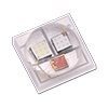
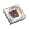
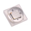
Fifth, packaging considerations
LED chip light also needs to go through the light guide and lens device, in order to improve the light extraction efficiency. In addition, heat dissipation is also very important to avoid heat to reduce luminous efficiency. Optimize the LED package structure to improve the final light-emitting effect is also very critical.